Semiconductor Components Manufacturer
As a specialized producer of semiconductor devices, we provide end-to-end solutions from wafer to packaged components. Our IATF 16949 certified facilities deliver products compliant with AEC-Q100 standards.
- 3,500+ semiconductor projects
- Semiconductor-grade packaging
- Advanced testing capabilities
- 48-hour sample delivery
- Full traceability systems
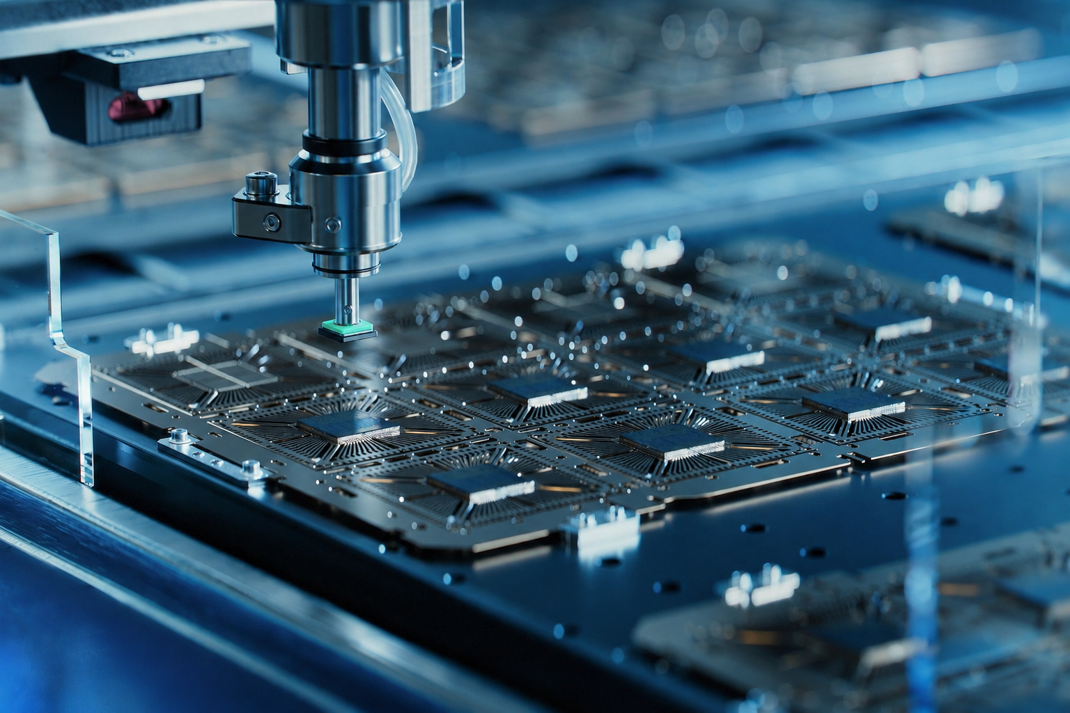
Custom Semiconductor Industry Parts and Products
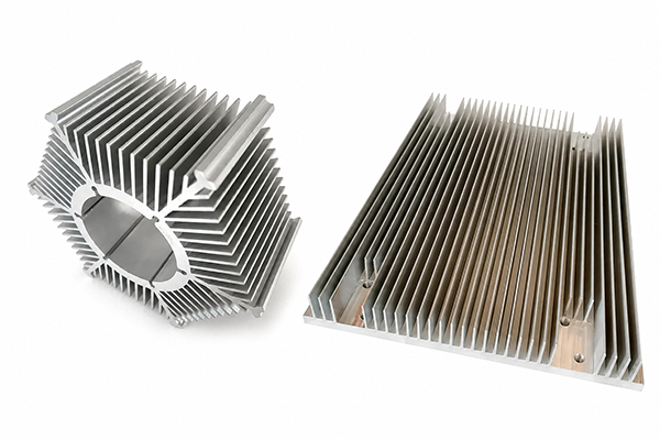
Aluminum Extrusion Heat Sink
Made of 6063 or 6061 aluminum alloy, it is processed by high temperature extrusion, CNC milling and drilling, and has surface treatments such as anodizing (hard/color) and sandblasting.
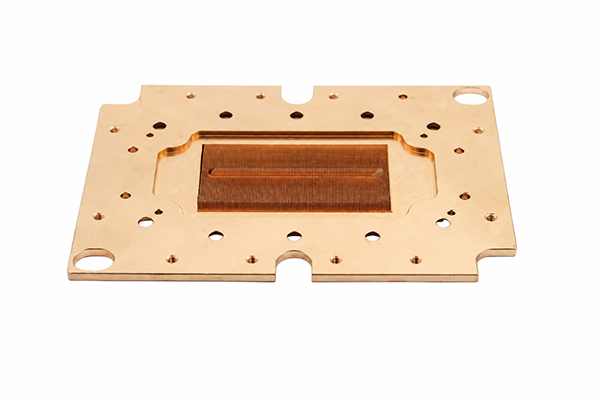
Microchannel Copper Cold Plate
The key components of CNC copper servers are usually made of high-conductivity oxygen-free copper or chromium-zirconium copper, and are formed through five-axis precision milling, slow wire cutting and diffusion welding processes.
Chamber Part
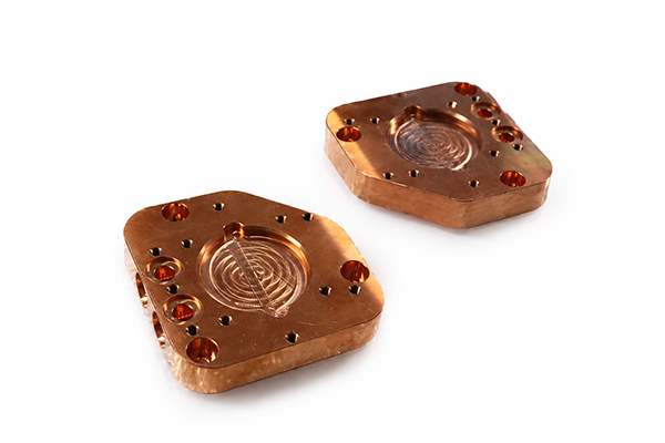
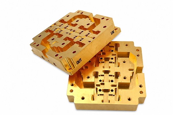
Copper CUP Block
Copper CUP Block is usually made of high-conductivity oxygen-free copper (OF-Cu, C10100) or tellurium copper (C14500) and processed by precision CNC turning (CNC), wire cutting (WEDM) or cold forging.
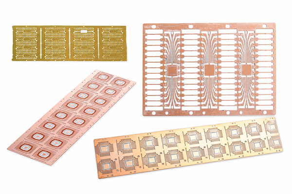
Copper Etched Semiconductor Lead Frame
Made of high-conductivity copper (C19400/C7025) or iron-copper alloy, formed by precision photochemical machining or high-speed stamping
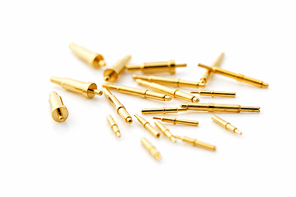
Copper Spring Probe
Made of beryllium copper alloy or phosphor bronze, processed by precision CNC turning, laser cutting or electrochemical etching, and selectively plated with gold, palladium nickel and other surface processes,
Semiconductor Part
Semiconductor parts are usually made of high-purity silicon, gallium arsenide or special alloys, manufactured through photolithography, etching, ion implantation, chemical mechanical polishing, plasma cleaning, etc.
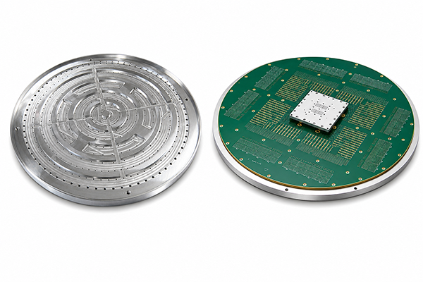
RF Shield Housing
RF shielding boxes are usually made of aluminum alloy (6061/5052), copper alloy (C11000) or galvanized steel sheet (SECC), and are manufactured through precision sheet metal stamping, CNC processing or die-casting.
Why Choose Bright Future for the Semiconductor?
Ultra-high cleanliness processing to meet the stringent requirements of semiconductor equipment
We uses Class 1000 dust-free workshop and oil-free cutting process to ensure that there is no metal dust and oil residue during the processing, and the surface cleanliness reaches ≤0.1mg/cm², which meets the ultra-high cleanliness standards of semiconductor equipment (such as wafer transfer manipulators and vacuum chambers).
Micron-level precision processing, suitable for precision semiconductor equipme
With five-axis ultra-precision CNC (precision ±0.003mm), key components in semiconductor equipment can be processed, such as EFEM frame, lithography machine positioning platform, vacuum valve, etc., to ensure nano-level motion accuracy and avoid wafer processing errors caused by micro-vibration.
Special material processing capability, corrosion resistance and high temperature resistance
Specialized in aluminum alloy (6061-T6), stainless steel (316L VM), ceramic composite materials and other semiconductor-specific materials, through mirror polishing (Ra≤0.1μm) and passivation treatment, to meet the long-term stability requirements in extreme environments such as high vacuum and plasma corrosion.
Anti-static and anti-pollution process
Adopt anti-static processing technology to avoid electrostatic adsorption particles during CNC process; all parts are cleaned by ultrasonic + plasma to ensure no residue, in line with SEMI F47 semiconductor equipment standards.
Fast delivery and strict traceability system
15-day rapid mass production: meet the urgent expansion needs of semiconductor equipment Laser coding + blockchain traceability: record material batches and processing parameters, support 10 years of data traceability, and comply with SEMI E142 standards
Successful cases in the semiconductor industry
Supplied to the world’s top 5 semiconductor equipment manufacturers, including: Wafer transfer robot: cumulative delivery of 100,000 sets, yield 99.99% Etcher chamber: processing accuracy ±0.005mm, plasma corrosion resistance life increased by 2 times Lithography machine structure: thermal deformation coefficient <0.001mm/℃, ensuring process stability below 28nm
Semiconductor
Provide pollution-proof, corrosion-resistant, ultra-high precision key component solutions for wafer equipment, etcher, photolithography machines, etc.
Wafer transfer robot
Vacuum chamber components
Etcher quartz ring
Photolithography machine guide rail
Stainless steel valve
CMP polishing head assembly